Introduction
Aims of the class
Introduce the basics of FPGA programming using Verilog on an Open Source and Free toolchain. Boards used will be the readily available Colorlite i5, which use the Lattice ECP5 FPGA. We will end with examples that utilize LiteX, which can be thought of as “IP cores” (but with more Python) and allow things like HDMI, ethernet, and even entire CPU cores to be synthesized in the FPGA.
You will not be an expert in FPGAs but you should be able to create simple programs and build more complex things over time.
This is not a class about learning how to use a computer or learning the deep intricacies of Verilog and LUTs. This is a practical class where you get your hands dirty trying to make your board do cool things. And we will sparkle a little bit of theory so you get a sense of what is happening.
Organization
The class will happen on May, 27th 2023 at PS1 and start promptly at 11AM, you can come a bit earlier if you think you need more time to setup.
Attention
You need to come with a computer already setup with all the tools. See the Requirements
This is the program of the day, this will obviously depends greatly on what you want to do, how fast you advance etc:
journey
title FPGA Class-Workshop
11AM Presentation of the participants and the class: 0
11.5AM What are FPGAs: 1
12AM First lessons: 2
01PM BYO Food break: 3
01.5PM Last cycle of the lessons: 5
03PM Hack your own stuff: 7
05PM Show your stuff: 9
So we will have a tiny formal introduction but we will jump really quickly into the practical work directly on your boards and you will learn things as you do.
The second part of the day will be about you hacking things together with the electronic components we have in the electronics area or the ones you or others did bring.
And the last part will be about you showing the group what you’ve achieved.
Disclaimer
We are not responsible for any damage, anywhere and on anything. You are connecting electronic devices to your computer and this comes with risks that you need to evaluate for yourself. Make sure you have backups and that you don’t use a computer that you can’t replace.
You are also going to install quite a lot of software from various places, so make sure you are using appropriate protections against the threats you fear the most.
Subsections of Requirements and setup
Linux setup (recommended)
Computer setup
You need a few things installed on your computer BEFORE THE CLASS:
- OSS-CAD
- Yosys
- A text editor you love and trust and are comfortable with
And you need to be able to setup your own networks (so no work locked computers) and install software from the internet (so no parental lock or other insanities).
Make sure you don’t try it for the first time on the day of the class, you will be unhappy and we will be as well.
Scripted installation on Debian/Ubuntu
wget -N  https://raw.githubusercontent.com/bjonnh/fpga_class_psone/main/setup_linux_admin.sh
chmod +x ./setup_linux_admin.sh
sudo ./setup_linux_admin.sh
# You will have to logout and login to get the new group pemissions.
wget -N  https://raw.githubusercontent.com/bjonnh/fpga_class_psone/main/setup_linux.sh
chmod +x ./setup_linux.sh
./setup_linux.sh
(Obviously you need curl installed and your user will need to be able to sudo)
Fast installation on other distros
You can follow most of the commands from:
https://raw.githubusercontent.com/bjonnh/fpga_class_psone/main/setup_linux.sh
Just replace apt/apt-get by what you use.
Linux details (useful only if you have issues or another distro)
Attention
You need to have cURL, git and other build tools installed.
And you need to be a member of the dialout group to be able to access the programmer serial port.
On ubuntu, those with:
sudo apt-get install build-essential curl git libhidapi-hidraw0
sudo usermod -a -G dialout,plugdev $USER
sudo curl -o /etc/udev/rules.d/99-openfpgaloader.rules https://raw.githubusercontent.com/trabucayre/openFPGALoader/master/99-openfpgaloader.rules
sudo udevadm control --reload-rules && sudo udevadm trigger # force udev to take new rule
# You will have to logout and login again
Go to
https://github.com/YosysHQ/oss-cad-suite-build/releases/tag/2023-05-05
and get the one for your platform, put it in /tmp
For example on x64, assuming you want to install in your home directory, it will decompress in ~/oss-cad-suite
This is assuming you will run all those commands in the same terminal.
# You can customize those, but you are responsible to change them when necessary
export DOWNLOADS_PATH=$HOME/Downloads
export INSTALL_PATH=$HOME

mkdir -p "$DOWNLOADS_PATH"
curl -L -o"$DOWNLOADS_PATH"/oss-cad-suite.tgz https://github.com/YosysHQ/oss-cad-suite-build/releases/download/2023-05-20/oss-cad-suite-linux-x64-20230520.tgz
tar -xzf "$DOWNLOADS_PATH"/oss-cad-suite.tgz --directory "$INSTALL_PATH"
cd "$INSTALL_PATH"/oss-cad-suite
source environment
Attention
Currently, the Python distributed with oss-cad doesn’t have the right version of pip
and remove the installed migen reference that conflicts with the one we will use for LiteX
MAKE SURE YOU RUN THE FOLLOWING COMMANDS, they work well on ubuntu, it will work ok on RedHat-like or Arch, but you will have to install the riscv toolchain yourself.
tabbypy3 -m pip install --upgrade pip
rm -rf lib/python3.*/site-packages/migen.egg-link
It will display something like:
Requirement already satisfied: pip in /home/you/Software/fpga/oss-cad-suite/lib/python3.8/site-packages (23.1.1)
Collecting pip
  Downloading pip-23.1.2-py3-none-any.whl (2.1 MB)
     ━━━━━━━━━━━━━━━━━━━━━━━━━━━━━━━━━━━━━━━━ 2.1/2.1 MB 30.4 MB/s eta 0:00:00
Installing collected packages: pip
  Attempting uninstall: pip
    Found existing installation: pip 23.1.1
    Uninstalling pip-23.1.1:
      Successfully uninstalled pip-23.1.1
Successfully installed pip-23.1.2
Install LiteX
This is really long, please make sure you do that BEFORE the day of the class.
mkdir -p litex
cd litex
curl -olitex_setup.py https://raw.githubusercontent.com/enjoy-digital/litex/master/litex_setup.py
tabbypy3 litex_setup.py --init --install
sudo python3 litex_setup.py --gcc=riscv
tabbypy3 -m pip install meson ninja
Testing it
cd "$INSTALL_PATH"/oss-cad-suite
mkdir -p projects
cd projects
git clone https://github.com/bjonnh/alscope
cd alscope
tabbypy3 ./main.py --ip-address=10.0.0.42 --build
If this failed you may not have enough memory to build FPGA programs… Or something failed during the installation
Usage
Now, anytime you need to use OSS-CAD:
export INSTALL_PATH=$HOME
source "$INSTALL_PATH"/oss-cad-suite/environment
This is all you need, any time you want to do something based on LiteX remember you have to use tabbypy3 and not python3 so you use the version that is packaged with oss-cad not the one from your OS.
MacOS setup
MacOS
Attention
You need to have a few tools installed.
We are giving instructions with brew, but if you know or use anything else, feel free to send us the commands to use.
It looks like that just installing brew installs all the tools necessary.
Go to
https://github.com/YosysHQ/oss-cad-suite-build/releases/tag/2023-05-05
and get the one for your platform, put it in /tmp
For example on x64, assuming you want to install in your home directory, it will decompress in ~/oss-cad-suite
(for M1 replace x64 by arm64)
This is assumed you will run all those commands in the same terminal.
# You can customize those, but you are responsible to change them when necessary
export DOWNLOADS_PATH=$HOME/Downloads
export INSTALL_PATH=$HOME
export ARCH=x64

mkdir -p "$DOWNLOADS_PATH"
curl -L -o"$DOWNLOADS_PATH"/oss-cad-suite.tgz https://github.com/YosysHQ/oss-cad-suite-build/releases/download/2023-05-05/oss-cad-suite-darwin-$ARCH-20230505.tgz
tar -xzf "$DOWNLOADS_PATH"/oss-cad-suite.tgz --directory "$INSTALL_PATH"
cd "$INSTALL_PATH"/oss-cad-suite
source environment
Attention
Currently, the Python distributed with oss-cad doesn’t have the right version of pip
and remove the installed migen reference that conflicts with the one we will use for LiteX
MAKE SURE YOU RUN THE FOLLOWING COMMANDS
tabbypy3 -m pip install --upgrade pip
rm -rf lib/python3.*/site-packages/migen.egg-link
It will display something like:
Requirement already satisfied: pip in /home/you/Software/fpga/oss-cad-suite/lib/python3.8/site-packages (23.1.1)
Collecting pip
  Downloading pip-23.1.2-py3-none-any.whl (2.1 MB)
     ━━━━━━━━━━━━━━━━━━━━━━━━━━━━━━━━━━━━━━━━ 2.1/2.1 MB 30.4 MB/s eta 0:00:00
Installing collected packages: pip
  Attempting uninstall: pip
    Found existing installation: pip 23.1.1
    Uninstalling pip-23.1.1:
      Successfully uninstalled pip-23.1.1
Successfully installed pip-23.1.2
Install LiteX
This is really long, please make sure you do that BEFORE the day of the class.
mkdir -p litex
cd litex
curl -olitex_setup.py https://raw.githubusercontent.com/enjoy-digital/litex/master/litex_setup.py
python3 litex_setup.py --init --install
cd ..
Unfortunately we don’t have instructions yet on how to setup the Risc V toolchain.
Testing it
cd "$INSTALL_PATH"/oss-cad-suite
mkdir -p projects
cd projects
git clone https://github.com/bjonnh/alscope
cd alscope
tabbypy3 ./main.py --ip-address=10.0.0.42 --build
If this failed you may not have enough memory to build FPGA programs… Or something failed during the installation
Usage
Now, anytime you need to use OSS-CAD:
export INSTALL_PATH=$HOME
source "$INSTALL_PATH"/oss-cad-suite/environment
This is all you need, any time you want to do something based on LiteX remember you have to use tabbypy3 and not python3 so you use the version that is packaged with oss-cad not the one from your OS.
Windows setup
Computer setup
You need a few things installed on your computer BEFORE THE CLASS:
- OSS-CAD
- Yosys
- A text editor you love and trust and are comfortable with
And you need to be able to setup your own networks (so no work locked computers) and install software from the internet (so no parental lock or other insanities).
Make sure you don’t try it for the first time on the day of the class, you will be unhappy and we will be as well.
Install on Windows
(This has only been tried on Windows 11 so far)
Windows doesn’t have everything
Certain tools like VHDL synthesis with GHDL only work on Linux and Mac, making you virtually only able to use Verilog or LiteX on windows unless you use WSL2 or a VM.
Making USB Jtag devices can also be somewhat tricky.
You need to install Git: https://git-scm.com/book/en/v2/Getting-Started-Installing-Git
(Looks like setting everything to the default except perhaps the editor is your best bet here).
Go to https://github.com/YosysHQ/oss-cad-suite-build/releases/tag/2023-05-05
And download the exe for Windows.
Run it. It will decompress … somewhere… And you can move it where you want it.
Once you are happy with that, open a powershell. Go to that directory and type
./start.bat
python3 -m pip install --upgrade pip
del .\lib\python3.8\site-packages\migen.egg-link
mkdir litex
cd litex
curl -olitex_setup.py https://raw.githubusercontent.com/enjoy-digital/litex/master/litex_setup.py # This is a single line starting with curl
python3 litex_setup.py --init --install
cd ..
mkdir projects
cd projects
git clone https://github.com/bjonnh/alscope
cd alscope
python3 ./main.py --ip-address=10.0.0.42 --build
JTAG programmer drivers
Windows is dumb with regard to drivers. You need to use a WinUSB driver for JTAG programmers (at least that’s the case with my DirtyJtag).
Follow the instructions at: https://learn.microsoft.com/en-us/windows-hardware/drivers/usbcon/winusb-installation
RISC v compiler suite
For this the easiest solution I found is to use MSYS2
and run inside msys2
pacman -S mingw-w64-x86_64-riscv64-unknown-elf-gcc ninja meson make
Then in your powershell
set PATH=%PATH%;C:\msys64\mingw64\bin;C:\msys64\usr\bin
But then I couldn’t get it to compile the board properly. So really you shouldn’t be using Windows… But we can still give you the files. Or you can help us fix that.
VM using VirtualBox
What we highly recommend for Windows and Mac users is to install a Ubuntu virtual machine, follow the Linux instructions and share the USB device with the VM.
Go to the settings of the VM, Ports, USB and add the JTAG device called NXP ARM mbed (0d28:0204) or something like that.
Subsections of Lessons
01 - Blink
Blinky is the “Hello world” of FPGAs
The code is in code/lesson_01
This is probably the simplest code you can use on an FPGA that will generate something you can see working.
How code is organized
Verilog
We have a verilog file. Verilog is a hardware description language that allows us to describe how we want the FPGA to react to specific logic signals.
module top(input clk_i, output led_o);
   reg  led_reg;
   wire baseclk;

   clkdiv #(.DIV(200000)) slowclk (clk_i, baseclk);

   always @(posedge baseclk) begin;
      led_reg <= ~led_reg;
   end

   assign led_o = led_reg;
endmodule


module clkdiv #(parameter DIV = 24'd5000)(
    input wire clk_i,
    output wire clk_o
    );

    reg [24:0] count = 25'b0;
    reg clk_o_internal = 1;
    //on this board we have a 25MHz clock

    always @(posedge clk_i) begin
        count <= count + 25'b1;
        if(count == DIV) begin
            count <= 25'b0;
            clk_o_internal <= ~clk_o_internal;
        end
    end
    assign clk_o = clk_o_internal;
endmodule
It looks scary but let’s try to decompose it
graph LR;
subgraph FPGA
clk_i;
led_o;
end
subgraph top
clk_i-->SOMETHING;
SOMETHING-->led_o;
end
We have some magic logic that takes a clk_i, transforms it and sends that to led_o.
LPF file
Now we also need to tell whatever will interpret that verilog, this is what clk_in and led_o are. That’s the role of the LPF file (Lattice Preference File), this file will link your human name to specific pins or internal lines inside the chip.
LOCATE COMP "clk_i" SITE "P3";
IOBUF PORT "clk_i" IO_TYPE=LVCMOS33;
FREQUENCY PORT "clk_i" 25 MHZ;

LOCATE COMP "led_o" SITE "U16";
IOBUF PORT "led_o" IO_TYPE=LVCMOS25;
We are taking the pad P3 of the FPGA (site definition), saying it has a 3V3 CMOS level (LVCMOS33) and that it is a frequency type port that’s receiving a 25MHz clock.
And we are saying the U16 is a 2.5V CMOS level (LVCMOS25) GPIO. This shouldn’t make sense since all the FPGA I/O banks (VCCIO pins) are supposedly connected to a 3.3V rail and therefore should be LVCMOS33 too. However, here we copied from other files but there are little reasons why this one was set to that.
Digging into “SOMETHING”
We will ignore the details of clkdiv for that lesson and do something people programming FPGA love: making abstractions and ignoring the implementation details! In practice unfortunately you often have to go dig in implementations for performance, size of power consumption reasons.
module top(input clk_i, output led_o);
   reg  led_reg;
   wire baseclk;

   clkdiv #(.DIV(200000)) slowclk (clk_i, baseclk);

   always @(posedge baseclk) begin;
      led_reg <= ~led_reg;
   end

   assign led_o = led_reg;
endmodule
Lets decypher that:
module top(input clk_i, output led_o);
endmodule
This is declaring a module named top (mandatory in Yosys, that’s the start of everything) that has one input clk_i and one output led_o. All things in Verilog are divided like that so blocks can be reused and reimplemented easily. You could think of them as “functions” for now (even if the reality is slightly more complex).
    reg led_reg;
    wire baseclk;
Here we are talking about two essential entities of Verilog, reg or registers which are ways to store information.
And wires which are how blocks are connected to each other.
The “input” and “output” above can also be specified as reg or wire but if not explicitly defined they are wire by default. i.e. input clk_i => input wire clk_i
clkdiv #(.DIV(200000)) slowclk (clk_i, baseclk);
Here we are instantiating a clkdiv block called slowclk. It takes clk_i and baseclk are what we call “nets” they are the connections to and from the module. And we set the parameter DIV to the value 200000. What this module does is dividing the input clock on clk_i by the DIV value and outputing that to baseclk. In our case clk_i is 25MHz, we divide by 200000 so we get a 125Hz output clock.
   always @(posedge baseclk) begin;
      led_reg <= ~led_reg;
   end
Now we are getting into the reality of FPGAs. Things are working in a synchronous way, but not as you see it in a computer where everything is directed by a single clock. In an FPGA you can have dozens or more clocks in your different modules, a single module can use multiple clocks etc. This the most difficult thing to grasp and solving clock issues is probably one of the major difficulty when working with FPGAs, because of latencies, potential inaccuracies of clocks (we will talk about that when using LiteX) and other issues.
Here we say, on the positive edge of baseclk, we want to assign to led_reg the inverse of its value (so if it was 0 it becomes 1 etc).
We have various kinds of assignment in Verilog and we have more details in the Candy jar - Assignments.
We will not get into the details here, just try to use non-blocking assignments inside your sequential (has either posedge or negedge) @always blocks to avoid race-conditions.
Here we say, at any time, led_o should take the value of led_reg. We are effectively connecting our register to the output of the FPGA.
Here is a representation of what we know so far:
graph LR;
subgraph FPGA
clk_i;
led_o;
end
subgraph top
clk_i;
subgraph CLKDIV["slowclk is_a clkdiv (DIV=200000)"]
magic;
end
baseclk-->PE{On posedge?};
PE -->|Yes| IV[Invert led_reg];
led_reg-->led_o;
end
clk_i-->CLKDIV;
CLKDIV-->baseclk;
Running the thing
We need quite a few steps to go from our Verilog description to something we can send to the FPGA.
graph TD;
Verilog --> S[[Synthesis\nYosys]];
S --> OD[Optimized design];
OD --> M[[Mapping\nYosys]];
M --> MD[Mapped design];
MD --> PR[[Place and Route\nnextpnr]];
PR --> PLD[Physical layout description];
PLD --> PK[[Generate flashable bitstream\necppack]];
PK --> Bitstream;
These are the commands you need to run to do those steps:
# blink.json is the optimized and mapped design
yosys -p "synth_ecp5 -top top -json blink.json" blink.v
# this will generate a placed and routed file blink_out.config
nextpnr-ecp5 --json blink.json --textcfg blink_out.config --25k --package CABGA381 --lpf blink.lpf
# this will generate both a SVF file and a bitstream BIT file
ecppack --compress --svf blink.svf blink_out.config blink.bit
A SVF (Serial Vector Format) file is a text file that describe the all the instructions that will be sent on the JTAG interface to program the chip. It is the way to transfer the Bitstream into the chip through its JTAG interface.
Currently we are just copying in a volatile way to the chip, cut the power and it is gone. There are ways to change the SVF file so it sends it to the connected FLASH instead (if it has one).
Sending to the board
If ecpdap is installed and working on your machine, you can use this to program the board:
Otherwise, openFPGALoader should do the trick:
sudo $HOME/oss-cad-suite/libexec/openFPGALoader -b "colorlight-i5" --freq "16000000" blink.svf
Exercice
02 - Repeat after me
We now want to talk to that FPGA. For that we have to declare an input:
LOCATE COMP "port_i" SITE "E1";
IOBUF PORT "port_i" PULLMODE=UP IO_TYPE=LVCMOS33;
Be really careful, the inputs on an FPGA are way more sensitive than on microcontrollers. Thankfully, really often you just burn that IO or a group of IOs so the FPGA still works but with less IOs.
Do not connect coils directly (relays, motors, speakers) and make sure you are using 3.3V logic (or lower if you defined lower in your LPF file) if you are connecting to something else.
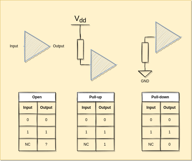
The FPGA contains pull-ups and pull-downs that you can set at synthesis time:
For more details on how the ECP5 handles the IOs see: https://www.latticesemi.com/-/media/LatticeSemi/Documents/ApplicationNotes/EH/FPGA-TN-02032-1-3-ECP5-ECP5G-sysIO-Usage-Guide.ashx?document_id=50464
Memory
In Verilog, you can create data types of arbitrary types:
This will create a register of SIZE bits called buffer.
To access a single bit, you use the bit index. Verilog uses zero-based indexing, so the least significant bit (LSB) is at index 0 and the most significant bit (MSB) is at index 7. For example, buffer[0] accesses the LSB of buffer, and buffer[SIZE-1] accesses the MSB.
To access a range of bits, you use a colon to specify the bit range. For example, buffer[3:0] accesses the least significant 4 bits of buffer, and buffer[7:4] accesses the most significant 4 bits (assuming SIZE=8 here).
We can set the value of a register at the beginning of the life of the module:
  initial begin
    buffer = 8'b01010101;
  end
Code
follow.lpf:
LOCATE COMP "clk_i" SITE "P3";
IOBUF PORT "clk_i" IO_TYPE=LVCMOS33;
FREQUENCY PORT "clk_i" 25 MHZ;

LOCATE COMP "led_o" SITE "U16";
IOBUF PORT "led_o" IO_TYPE=LVCMOS25;

LOCATE COMP "port_i" SITE "E1";
IOBUF PORT "port_i" PULLMODE=UP IO_TYPE=LVCMOS33;
follow.v
module top(input clk_i, input port_i, output led_o);
   reg  led_reg;
   wire baseclk;

   clkdiv #(.DIV(200000)) slowclk (clk_i, baseclk);
   ring_buffer  buffer (baseclk, port_i, led_o);
endmodule


module ring_buffer (
  input wire clk,
  input wire data_in,
  output wire data_out
);
  reg [255:0] buffer;
  reg [7:0]   write_pointer;
  reg [7:0]   read_pointer;

  initial begin
    buffer = 256'b0000000000000000000000000000000000000000000011111111000000001111111100000000111111110000000011111111111111110000000011111111111111110000000011111111111111110000000011111111000000001111111100000000111111110000000000000000000000000000000000000000000000000000;
  end

  always @(posedge clk) begin
    buffer[write_pointer] <= data_in;
    write_pointer <= write_pointer + 1;
    read_pointer  <= read_pointer + 1;
  end

  assign data_out = buffer[read_pointer];

endmodule


module clkdiv #(parameter DIV = 24'd5000)(
    input wire clk_i,
    output wire clk_o
    );

    reg [24:0] count = 25'b0;
    reg clk_o_internal = 1;
    //on this board we have a 25MHz clock

    always @(posedge clk_i) begin
        count <= count + 25'b1;
        if(count == DIV) begin
            count <= 25'b0;
            clk_o_internal <= ~clk_o_internal;
        end
    end
    assign clk_o = clk_o_internal;
endmodule
Build
yosys -p "synth_ecp5 -top top -json follow.json" follow.v
nextpnr-ecp5 --json follow.json --textcfg follow.config --25k --package CABGA381 --lpf follow.lpf
ecppack --compress --svf follow.svf follow.config follow.bit
Upload
ecpdap program follow.bit
sudo $HOME/oss-cad-suite/libexec/openFPGALoader -b "colorlight-i5" --freq "16000000" follow.svf
Exercice
03 - LiteX
Using high-level languages to describe systems offers several significant advantages. They abstract away many low-level details, making the design process more intuitive and efficient. This abstraction allows designers to focus on the system’s functionality and architecture, rather than getting bogged down in the minutiae of hardware specifics. High-level languages also tend to be more expressive and readable than low-level languages, facilitating better understanding and communication among team members. Furthermore, they often come with extensive standard libraries and tools, enabling rapid prototyping and debugging. Lastly, high-level languages allow for the use of advanced software engineering practices, such as object-oriented programming and automated testing, leading to more reliable and maintainable systems (well that is the theory at least).
Migen and LiteX
Migen is a Python-based tool that aims to make digital design (including both ASIC and FPGA design) more efficient and enjoyable (yay). It was developed by the M-Labs team as an improvement over existing hardware description languages (HDLs) such as VHDL and Verilog.
Migen introduces several novel concepts and adopts many good ones from existing HDLs. It also leverages the capabilities of Python as a powerful and expressive high-level language, enabling you to write more compact, maintainable, and reusable digital designs.
Key features of Migen include:
- Fragmented Hardware Description: Migen allows hardware designs to be split into fragments that can be combined and transformed.
- Powerful Language Constructs: Migen provides powerful language constructs like generators and list comprehensions, which can simplify and improve the readability of complex hardware designs.
- Python-based: As a Python-based tool, Migen allows you to use Python’s extensive standard library and third-party modules, making it easier to develop and test hardware designs.
- Built-in Simulation: Migen includes a built-in simulation environment that allows you to test your designs without needing external tools.
- FPGA Flow Management: Migen includes the MiSoC project (now called LiteX), which provides a high-level way to design system-on-chip solutions, manage the FPGA flow, and handle on-chip interconnects.
Learning Migen may require learning Python if you are not already familiar with it. However, for those comfortable with Python, Migen can provide a powerful and flexible toolset for digital design.
LiteX is an open-source Python library that provides a high-level, hardware-agnostic interface for developing digital designs for FPGAs. It was created by the Enjoy Digital team and is widely used in the FPGA community. LiteX simplifies the process of designing and deploying digital designs on FPGAs by abstracting away many of the low-level details that are often required when working directly with FPGA hardware.
LiteX includes various components that help in the development of FPGA projects, such as:
- Core: A Python library that provides a high-level API for describing digital circuits.
- SoC: An SoC (System-on-Chip) builder that allows you to create and integrate custom SoCs with various peripherals and soft processor cores.
- BIOS: A minimal BIOS for LiteX SoCs, which helps in the initial configuration and testing of the hardware.
- Build tools: A set of tools that assist in the generation of FPGA bitstreams, including wrappers for various FPGA synthesis and place-and-route tools (such as Yosys and NextPNR).
LiteX can be used with a wide range of FPGA devices and development boards, including the Lattice ECP5 that is on your board. The library is also compatible with several soft processor cores, like RISC-V and LM32, allowing users to create custom SoCs tailored to their specific needs.
Example: An ethernet logic-analyzer in a few lines of Python
Create a file main.py
#!/usr/bin/env python3

#
# This file is based on Colorlite (https://github.com/enjoy-digital/colorlite)
#
# Copyright (c) 2020-2022 Florent Kermarrec <florent@enjoy-digital.fr>
# Copyright (c) 2023 Jonathan Bisson <bjonnh-github@bjonnh.net>
# SPDX-License-Identifier: BSD-2-Clause

from liteeth.phy.ecp5rgmii import LiteEthPHYRGMII
from litescope import LiteScopeAnalyzer
from litex.build.generic_platform import *
from litex.soc.cores.clock import *
from litex.soc.cores.gpio import GPIOOut
from litex.soc.cores.led import LedChaser
from litex.soc.cores.spi_flash import ECP5SPIFlash
from litex.soc.integration.builder import *
from litex.soc.integration.soc_core import *
from litex_boards.platforms import colorlight_i5
from migen import *
from migen.genlib.misc import WaitTimer

# IOs ----------------------------------------------------------------------------------------------

#_gpios = [
#    # GPIOs.
#    ("gpio", 0, Pins("j4:0"), IOStandard("LVCMOS33")),
#    ("gpio", 1, Pins("j4:1"), IOStandard("LVCMOS33")),
#]


# CRG ----------------------------------------------------------------------------------------------

class _CRG(Module):
    def __init__(self, platform, sys_clk_freq):
        self.clock_domains.cd_sys = ClockDomain()
        # # #

        # Clk / Rst.
        clk25 = platform.request("clk25")
        #rst_n = platform.request("user_btn_n", 0)

        # PLL.
        self.submodules.pll = pll = ECP5PLL()
        #self.comb += pll.reset.eq(~rst_n)
        pll.register_clkin(clk25, 25e6)
        pll.create_clkout(self.cd_sys, sys_clk_freq)


# ColorLite ----------------------------------------------------------------------------------------

class ColorLite(SoCMini):
    def __init__(self, sys_clk_freq=int(50e6), with_etherbone=True, ip_address=None, mac_address=None):
        platform = colorlight_i5.Platform(revision="7.0")

        # CRG --------------------------------------------------------------------------------------
        self.submodules.crg = _CRG(platform, sys_clk_freq)

        # SoCMini ----------------------------------------------------------------------------------
        SoCMini.__init__(self, platform, clk_freq=sys_clk_freq)

        # Etherbone --------------------------------------------------------------------------------
        if with_etherbone:
            self.submodules.ethphy = LiteEthPHYRGMII(
                clock_pads=self.platform.request("eth_clocks"),
                pads=self.platform.request("eth"),
                tx_delay=0e-9)
            self.add_etherbone(
                phy=self.ethphy,
                ip_address=ip_address,
                mac_address=mac_address,
                data_width=32,
            )

        # artificial signal
        count = Signal(8)
        #rst_n = platform.request("user_btn_n", 0)
        self.sync += count.eq(count + 1)
        analyzer_signals = [
            count,
        #    rst_n
        ]
        self.submodules.analyzer = LiteScopeAnalyzer(analyzer_signals,
            depth=1024,
            clock_domain="sys",
            samplerate=self.sys_clk_freq,
            csr_csv="analyzer.csv"
        )
        self.add_csr("analyzer")

        # GPIOs ------------------------------------------------------------------------------------
        #platform.add_extension(_gpios)

        # Power switch
        #power_sw_pads = platform.request("gpio", 0)
        #power_sw_gpio = Signal()
        #power_sw_timer = WaitTimer(2 * sys_clk_freq)  # Set Power switch high after power up for 2s.
        #self.comb += power_sw_timer.wait.eq(1)
        #self.submodules += power_sw_timer
        ##self.submodules.gpio0 = GPIOOut(power_sw_gpio)
        #self.comb += power_sw_pads.eq(power_sw_gpio | ~power_sw_timer.done)

        # Reset Switch
        #reset_sw_pads = platform.request("gpio", 1)
        #self.submodules.gpio1 = GPIOOut(reset_sw_pads)


# Build --------------------------------------------------------------------------------------------

def main():
    parser = argparse.ArgumentParser(description="Take control of your ColorLight FPGA board with LiteX/LiteEth :)")
    parser.add_argument("--build", action="store_true", help="Build bitstream")
    parser.add_argument("--load", action="store_true", help="Load bitstream")
    parser.add_argument("--ip-address", default="10.0.0.42",
                        help="Ethernet IP address of the board (default: 10.0.0.42).")
    parser.add_argument("--mac-address", default="0x726b895bc2e2",
                        help="Ethernet MAC address of the board (defaullt: 0x726b895bc2e2).")
    args = parser.parse_args()

    soc = ColorLite(ip_address=args.ip_address, mac_address=int(args.mac_address, 0))
    builder = Builder(soc, output_dir="build", csr_csv="csr.csv")
    builder.build(build_name="colorlite", run=args.build)

    if args.load:
        prog = soc.platform.create_programmer()
        prog.load_bitstream(os.path.join(builder.gateware_dir, soc.build_name + ".bit"))

if __name__ == "__main__":
    main()
Build
Upload
We are supposed to be able to do:
ecpdap program build/gateware/colorlite.bit
To load on the board but it doesn’t always work.
In which case you should do:
sudo $HOME/oss-cad-suite/libexec/openFPGALoader -b "colorlight-i5" --freq "16000000" ./build/gateware/colorlite.svf
Run
Check that you can ping your board (edit the main.py file and rebuild if you don’t like the default IP)
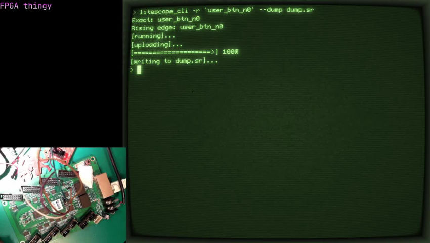
Run the litex server
litex_server --udp --udp-ip=10.0.0.42
Start an acquisition:
litescope_cli --dump dump.sr
It will trigger the logic analyzer and save a file dump.sr with the signals. You can also do a .csv by changing dump.sr by dump.csv.
You can view it using tools like sigrok-cli or gtkwave:
sigrok-cli -i dump.sr -O ascii
You can see a demo video below:
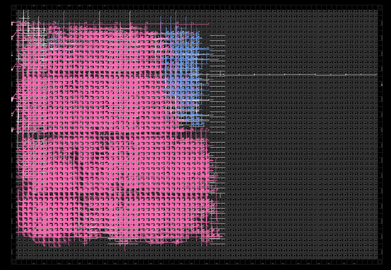
How much does it take on the chip
In pink, ethernet, in blue the analyzer and its memory.
Exercice
This one is hard and will require you to read this documentation: https://github.com/enjoy-digital/litex/wiki/Reuse-a-(System)Verilog,-VHDL,-(n)Migen,-Spinal-HDL,-Chisel-core
04 - Blink...again?
Tri-state buffers
Logic states in verilog can not only take on the binary values of one and zero, but there is a valid “third” state called high-Z (or high impedance). This is a fancy way of saying disconnect something completely, i.e. an open circuit.
To highlight this, let’s take a 1-bit wire that is presumably connected to an output pin with nothing else connected to it. We can set it to any of these 1-bit constants.
wire tri_test = 1'b0;	// the voltage at this pin would be 0 volts
wire tri_test = 1'b1;	// the voltage here would be 3.3 volts
wire tri_test = 1'bz;	// voltage here...is not well defined; the pin is "floating"
This is called a tri-state buffer. These are typically used on bidirectional data buses with one or more devices attached. When a single device on the bus wants to put data out onto the bus, all the other connected devices must put their data lines into “high-Z”, or put another way, “tri-state” their outputs.
If they don’t do this properly, then the bus is in “contention” and can result in funky operation and/or damage. The opposite can also happen where the bus is completely floating and can give erronous
values unless something “pulls” it up/down to a high/low state.
Although using z in verilog is perfectly valid, the Yosys open-source synthesis tools currently don’t support translating something like 1'bz onto a GPIO pin. You’ll get a warning that looks like this:
Warning: Yosys has only limited support for tri-state logic at the moment.
However, since verilog is only our higher level “C code” for describing FPGA behavior, we can drop down to use the “inline assembly” of describing this same behavior.
The language FPGAs use for its low-level building blocks are called the “device primitives”. Lattice has a document describing the primitives for many of its FPGA devices and it can be found here.
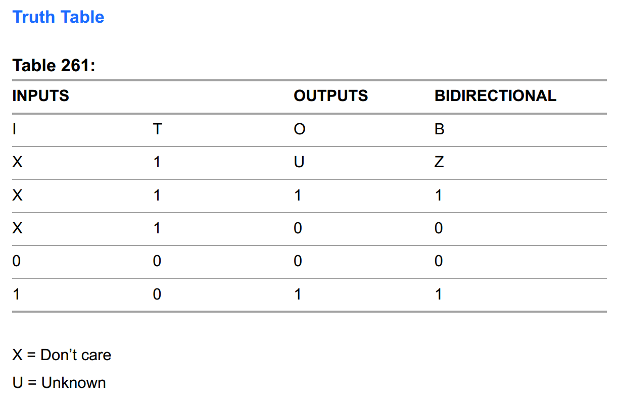
We’re interested in the BB primitive which they call “CMOS Input 6mA Sink 3mA Source Sinklim Output Buffer with Tristate – BiDirectional”. They give the following schematic representation and truth table:
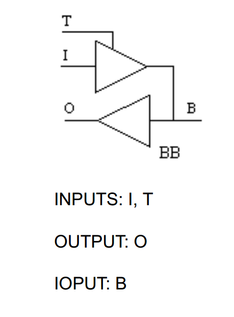
If we want to instantiate this primitve in our code, the sysI/O usage guide gives a verilog example as such:
BB buf7 (.I(Q_out7), .T(Q_tri7), .O(buf_Data7), .B(Data[7]));
This wasn’t covered previously, but when instantiating a module (any module) you can list the instance ports in the same order as the module definition. Or you can do what they did here where the port name within the module is called out with a dot in front of it and the instance port is in parentheses next to it. This creates a mapping where things can be out of order, or you can leave unused ports out if you don’t need them. It also reduces the chance of making a mistake in the ordering.
Finite state machines
Building a state machine is a fundamental exercise in FPGA design. All CPUs use some kind of state machine as the basis of how they operate and execute instructions.
The clock signal moves the machine forward through its states
We first need to define our states and describe how we want to allow them to move between each other. We’ll make a project where we hook up a single GPIO pin (FPGA-pad K5 as coded in this example) as such:
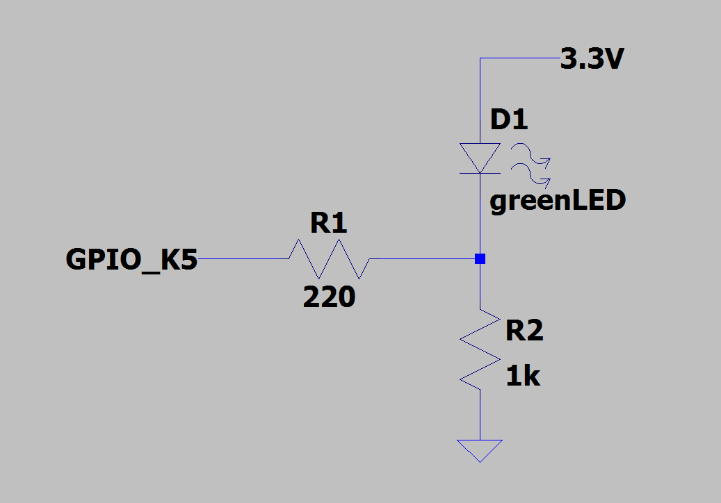
and we’ll make that pin a tri-state output and define all three states. When the pin is a one (3.3V), the LED should turn off completely because all the current is flowing between the pin and ground, i.e. we’re shorting across the LED.
When the pin is a zero (0V), the LED is on and quite bright because current flows through the parallel combination of both resistors (~180ohm) since they’re both connected to 0V (ground).
And finally, when the pin is high-Z it is disconnected so the LED is still on but current is only flowing through the 1k resistor and will therefore be much dimmer. So we have three states we can move between.
localparam state_off = 2'b00;
localparam state_dim = 2'b01;
localparam state_brite = 2'b10;
reg [1:0] led_state = state_off;
The localparam keyword is typicaly a good choice for defining constant values within a module. There are other ways but we won’t cover them now.
Since there are 3 valid states, we need at least two bits to cover that many states. Therefore, our defined states and state register are all 2-bits.
We’ll use a clock for this state machine which yields us a 100ms period, so we divide the 25MHz by 2500000:
clkdiv #(.DIV(2500000)) slowclk(
	.clk_i(clk),
	.clk_o(baseclk));
Lastly, we want to be able to control how long we’re in each state. To keep it simple, we’ll use the same time between each state.
localparam state_time = 5;
reg [7:0] counter = state_time;
The best way to manage our states is to use the verilog case statement.
Our state register is the “expression” for the case, and our predefined state names are what’s populated for each case. It’s important to populate the default case so the machine never gets “stuck”.
So we’ll just copy the code for state_off into default.
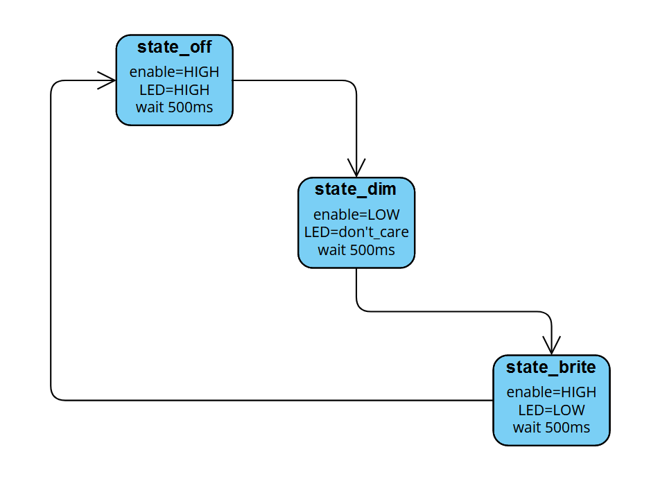
The state machine is structured such that the initial state is off, then it proceeds to the dim state, and then the bright state before it loops back to the off state and repeats indefinitely.
The enable register is what we use to put the output into the high-Z state. When enable is high, we don’t care what led is set to. The following diagram shows a visual representation of this very basic state machine.
The Code
At this point, let’s just see the code in its entirety:
blink_zed.v
module top(input wire clk, output wire led_pin);
	wire baseclk;
	reg led;
	reg enable;

	// set up state names and initialize the state
	localparam state_off = 2'b00;
	localparam state_dim = 2'b01;
	localparam state_brite = 2'b10;
	reg [1:0] led_state = state_off;

	// divide input 25MHz clock to get a period of 100ms (10Hz)
	clkdiv #(.DIV(2500000)) slowclk(
			.clk_i(clk),
			.clk_o(baseclk));

	// set up delay counter for the state machine
	// each clock period is 100ms so total wait time is 500ms
	localparam state_time = 5;
	reg [7:0] counter = state_time;

	// the actual state machine
	always @(posedge baseclk) begin
	case (led_state)
		state_off: begin
			enable = 1'b1;
			led <= 1'b1;
			counter <= counter - 1;
			if (counter == 0) begin
				counter <= state_time;
				led_state <= state_dim;
			end
		end
		state_dim: begin
			enable = 1'b0;
			led <= 1'b1;
			counter <= counter - 1;
			if (counter == 0) begin
				counter <= state_time;
				led_state <= state_brite;
			end
		end
		state_brite: begin
			enable = 1'b1;
			led <= 1'b0;
			counter <= counter - 1;
			if (counter == 0) begin
				counter <= state_time;
				led_state <= state_off;
			end
		end
		default: begin
			enable = 1'b1;
			led <= 1'b1;
			counter <= counter - 1;
			if (counter == 0) begin
				counter <= state_time;
				led_state <= state_dim;
			end
		end
	endcase
	end

	// primitive for bi-directional buffer which allows tri-stating
	BB tristate_out (.I(led), .T(~enable), .B(led_pin));

endmodule


module clkdiv #(parameter DIV = 24'd5000)(
    input wire clk_i,
    output wire clk_o
    );

    reg [24:0] count = 25'b0;
    reg clk_o_internal = 1;
    //on this board we have a 25MHz clock

    always @(posedge clk_i) begin
        count <= count + 25'b1;
        if(count == DIV) begin
            count <= 25'b0;
            clk_o_internal <= ~clk_o_internal;
        end
    end
    assign clk_o = clk_o_internal;
endmodule
The only portion of the above code not fully discussed yet is the BB tristate_out instance. A couple things to note.
First, the T port is like an active-low enable input, so our enable signal is being inverted with the leading tilde (~) character.
Also worth mentioning is that the O port is not used here so we don’t have to connect anything to it.
blink_zed.lpf
LOCATE COMP "clk" SITE "P3";
IOBUF PORT "clk" IO_TYPE=LVCMOS33;
FREQUENCY PORT "clk" 25 MHZ;

LOCATE COMP "led_pin" SITE "K5";
IOBUF PORT "led_pin" IO_TYPE=LVCMOS33 DRIVE=12;
A bonus tidbit here is the DRIVE attribute which sets the drive strength of an output pin. There is much more info in the the sysI/O usage guide, but the general jist of it is that you can set it between 4, 8, 12, and 16. What this does in practice is change the ON resistance of the transistors driving the output. A higher value of drive strength results in lower ON resistance, which means the effective series resistance of your output is lower and therefore you can push/pull more current out/in of the pin while maintaining valid logic levels at the receiving device(s).
Build
yosys -p "synth_ecp5 -top top -json blink_zed.json" blink_zed.v
nextpnr-ecp5 --json blink_zed.json --textcfg blink_zed_out.config --25k --package CABGA381 --lpf blink_zed.lpf
ecppack --compress --svf blink_zed.svf blink_zed_out.config blink_zed.bit
Upload
ecpdap program blink_zed.bit
OR
sudo $HOME/oss-cad-suite/libexec/openFPGALoader -b "colorlight-i5" --freq "16000000" blink_zed.svf
Exercice
05 - LiteX for real
LiteX can do a lot more than our previous example. It was created to generate SoC (systems on chips) that can be configured.
For this lesson to work you will have to install a Risc V compiler.
Create a file colorlight_i5.py:
#!/usr/bin/env python3

#
# This file is part of LiteX-Boards.
#
# Copyright (c) 2021 Kazumoto Kojima <kkojima@rr.iij4u.or.jp>
# SPDX-License-Identifier: BSD-2-Clause

from migen import *

from litex.gen import *

from litex.build.io import DDROutput

from litex_boards.platforms import colorlight_i5

from litex.soc.cores.clock import *
from litex.soc.integration.soc_core import *
from litex.soc.integration.builder import *
from litex.soc.cores.video import VideoHDMIPHY
from litex.soc.cores.led import LedChaser

from litex.soc.interconnect.csr import *

from litedram.modules import M12L64322A # Compatible with EM638325-6H.
from litedram.phy import GENSDRPHY, HalfRateGENSDRPHY

from liteeth.phy.ecp5rgmii import LiteEthPHYRGMII

# CRG ----------------------------------------------------------------------------------------------

class _CRG(LiteXModule):
    def __init__(self, platform, sys_clk_freq, use_internal_osc=False, with_usb_pll=False, with_video_pll=False, sdram_rate="1:1"):
        self.rst    = Signal()
        self.cd_sys = ClockDomain()
        if sdram_rate == "1:2":
            self.cd_sys2x    = ClockDomain()
            self.cd_sys2x_ps = ClockDomain()
        else:
            self.cd_sys_ps = ClockDomain()

        # # #

        # Clk / Rst
        if not use_internal_osc:
            clk = platform.request("clk25")
            clk_freq = 25e6
        else:
            clk = Signal()
            div = 5
            self.specials += Instance("OSCG",
                p_DIV = div,
                o_OSC = clk
            )
            clk_freq = 310e6/div

        rst_n = platform.request("cpu_reset_n")

        # PLL
        self.pll = pll = ECP5PLL()
        self.comb += pll.reset.eq(~rst_n | self.rst)
        pll.register_clkin(clk, clk_freq)
        pll.create_clkout(self.cd_sys,    sys_clk_freq)
        if sdram_rate == "1:2":
            pll.create_clkout(self.cd_sys2x,    2*sys_clk_freq)
            pll.create_clkout(self.cd_sys2x_ps, 2*sys_clk_freq, phase=180) # Idealy 90° but needs to be increased.
        else:
           pll.create_clkout(self.cd_sys_ps, sys_clk_freq, phase=180) # Idealy 90° but needs to be increased.

        # USB PLL
        if with_usb_pll:
            self.usb_pll = usb_pll = ECP5PLL()
            self.comb += usb_pll.reset.eq(~rst_n | self.rst)
            usb_pll.register_clkin(clk, clk_freq)
            self.cd_usb_12 = ClockDomain()
            self.cd_usb_48 = ClockDomain()
            usb_pll.create_clkout(self.cd_usb_12, 12e6, margin=0)
            usb_pll.create_clkout(self.cd_usb_48, 48e6, margin=0)

        # Video PLL
        if with_video_pll:
            self.video_pll = video_pll = ECP5PLL()
            self.comb += video_pll.reset.eq(~rst_n | self.rst)
            video_pll.register_clkin(clk, clk_freq)
            self.cd_hdmi   = ClockDomain()
            self.cd_hdmi5x = ClockDomain()
            video_pll.create_clkout(self.cd_hdmi,    40e6, margin=0)
            video_pll.create_clkout(self.cd_hdmi5x, 200e6, margin=0)

        # SDRAM clock
        sdram_clk = ClockSignal("sys2x_ps" if sdram_rate == "1:2" else "sys_ps")
        self.specials += DDROutput(1, 0, platform.request("sdram_clock"), sdram_clk)

# BaseSoC ------------------------------------------------------------------------------------------

class BaseSoC(SoCCore):
    def __init__(self, board="i5", revision="7.0", toolchain="trellis", sys_clk_freq=60e6,
        with_ethernet          = False,
        with_etherbone         = False,
        local_ip               = "",
        remote_ip              = "",
        eth_phy                = 0,
        with_led_chaser        = True,
        use_internal_osc       = False,
        sdram_rate             = "1:1",
        with_video_terminal    = False,
        with_video_framebuffer = False,
        **kwargs):
        board = board.lower()
        assert board in ["i5", "i9"]
        platform = colorlight_i5.Platform(board=board, revision=revision, toolchain=toolchain)

        # CRG --------------------------------------------------------------------------------------
        with_usb_pll   = kwargs.get("uart_name", None) == "usb_acm"
        with_video_pll = with_video_terminal or with_video_framebuffer
        self.crg = _CRG(platform, sys_clk_freq,
            use_internal_osc = use_internal_osc,
            with_usb_pll     = with_usb_pll,
            with_video_pll   = with_video_pll,
            sdram_rate       = sdram_rate
        )

        # SoCCore ----------------------------------------------------------------------------------
        SoCCore.__init__(self, platform, int(sys_clk_freq), ident = "LiteX SoC on Colorlight " + board.upper(), **kwargs)

        # Leds -------------------------------------------------------------------------------------
        if with_led_chaser:
            ledn = platform.request_all("user_led_n")
            self.leds = LedChaser(pads=ledn, sys_clk_freq=sys_clk_freq)

        # SPI Flash --------------------------------------------------------------------------------
        if board == "i5":
            from litespi.modules import GD25Q16 as SpiFlashModule
        if board == "i9":
            from litespi.modules import W25Q64 as SpiFlashModule

        from litespi.opcodes import SpiNorFlashOpCodes as Codes
        self.add_spi_flash(mode="1x", module=SpiFlashModule(Codes.READ_1_1_1))

        # SDR SDRAM --------------------------------------------------------------------------------
        if not self.integrated_main_ram_size:
            sdrphy_cls = HalfRateGENSDRPHY if sdram_rate == "1:2" else GENSDRPHY
            self.sdrphy = sdrphy_cls(platform.request("sdram"))
            self.add_sdram("sdram",
                phy           = self.sdrphy,
                module        = M12L64322A(sys_clk_freq, sdram_rate),
                l2_cache_size = kwargs.get("l2_size", 8192)
            )

        # Ethernet / Etherbone ---------------------------------------------------------------------
        if with_ethernet or with_etherbone:
            self.ethphy = LiteEthPHYRGMII(
                clock_pads = self.platform.request("eth_clocks", eth_phy),
                pads       = self.platform.request("eth", eth_phy),
                tx_delay = 0)
            if with_ethernet:
                self.add_ethernet(phy=self.ethphy)
            if with_etherbone:
                self.add_etherbone(phy=self.ethphy)

        if local_ip:
            local_ip = local_ip.split(".")
            self.add_constant("LOCALIP1", int(local_ip[0]))
            self.add_constant("LOCALIP2", int(local_ip[1]))
            self.add_constant("LOCALIP3", int(local_ip[2]))
            self.add_constant("LOCALIP4", int(local_ip[3]))

        if remote_ip:
            remote_ip = remote_ip.split(".")
            self.add_constant("REMOTEIP1", int(remote_ip[0]))
            self.add_constant("REMOTEIP2", int(remote_ip[1]))
            self.add_constant("REMOTEIP3", int(remote_ip[2]))
            self.add_constant("REMOTEIP4", int(remote_ip[3]))

        # Video ------------------------------------------------------------------------------------
        if with_video_terminal or with_video_framebuffer:
            self.videophy = VideoHDMIPHY(platform.request("gpdi"), clock_domain="hdmi")
            if with_video_terminal:
                self.add_video_terminal(phy=self.videophy, timings="800x600@60Hz", clock_domain="hdmi")
            if with_video_framebuffer:
                self.add_video_framebuffer(phy=self.videophy, timings="800x600@60Hz", clock_domain="hdmi")

# Build --------------------------------------------------------------------------------------------

def main():
    from litex.build.parser import LiteXArgumentParser
    parser = LiteXArgumentParser(platform=colorlight_i5.Platform, description="LiteX SoC on Colorlight I5.")
    parser.add_target_argument("--board",            default="i5",             help="Board type (i5).")
    parser.add_target_argument("--revision",         default="7.0",            help="Board revision (7.0).")
    parser.add_target_argument("--sys-clk-freq",     default=60e6, type=float, help="System clock frequency.")
    ethopts = parser.target_group.add_mutually_exclusive_group()
    ethopts.add_argument("--with-ethernet",   action="store_true",      help="Enable Ethernet support.")
    ethopts.add_argument("--with-etherbone",  action="store_true",      help="Enable Etherbone support.")
    parser.add_target_argument("--remote-ip", default="192.168.1.100",  help="Remote IP address of TFTP server.")
    parser.add_target_argument("--local-ip",  default="192.168.1.50",   help="Local IP address.")
    sdopts = parser.target_group.add_mutually_exclusive_group()
    sdopts.add_argument("--with-spi-sdcard",  action="store_true", help="Enable SPI-mode SDCard support.")
    sdopts.add_argument("--with-sdcard",      action="store_true", help="Enable SDCard support.")
    parser.add_target_argument("--eth-phy",          default=0, type=int, help="Ethernet PHY (0 or 1).")
    parser.add_target_argument("--use-internal-osc", action="store_true", help="Use internal oscillator.")
    parser.add_target_argument("--sdram-rate",       default="1:1",       help="SDRAM Rate (1:1 Full Rate or 1:2 Half Rate).")
    viopts = parser.target_group.add_mutually_exclusive_group()
    viopts.add_argument("--with-video-terminal",    action="store_true", help="Enable Video Terminal (HDMI).")
    viopts.add_argument("--with-video-framebuffer", action="store_true", help="Enable Video Framebuffer (HDMI).")
    args = parser.parse_args()

    soc = BaseSoC(board=args.board, revision=args.revision,
        toolchain              = args.toolchain,
        sys_clk_freq           = args.sys_clk_freq,
        with_ethernet          = args.with_ethernet,
        with_etherbone         = args.with_etherbone,
        local_ip               = args.local_ip,
        remote_ip              = args.remote_ip,
        eth_phy                = args.eth_phy,
        use_internal_osc       = args.use_internal_osc,
        sdram_rate             = args.sdram_rate,
        with_video_terminal    = args.with_video_terminal,
        with_video_framebuffer = args.with_video_framebuffer,
        **parser.soc_argdict
    )
    soc.platform.add_extension(colorlight_i5._sdcard_pmod_io)
    if args.with_spi_sdcard:
        soc.add_spi_sdcard()
    if args.with_sdcard:
        soc.add_sdcard()

    builder = Builder(soc, **parser.builder_argdict)
    if args.build:
        builder.build(**parser.toolchain_argdict)

    if args.load:
        prog = soc.platform.create_programmer()
        prog.load_bitstream(builder.get_bitstream_filename(mode="sram"))

if __name__ == "__main__":
    main()
Build
python3 colorlight_i5.py --ecppack-compress --build
Upload
ecpdap program build/gateware/colorlite.bit
(We could have used –load but there is a bug in Litex)
If your ecpdap works
Or:
openFPGALoader -b "colorlight-i5" --freq "16000000" ./build/colorlight_i5/gateware/colorlight_i5.svf
Connect using the serial terminal
On Linux:
On windows I do not know at all.
Once you are inside press enter you should see:
Now:
litex> reboot
        __   _ __      _  __
       / /  (_) /____ | |/_/
      / /__/ / __/ -_)>  <
     /____/_/\__/\__/_/|_|
   Build your hardware, easily!

 (c) Copyright 2012-2023 Enjoy-Digital
 (c) Copyright 2007-2015 M-Labs

 BIOS built on May 19 2023 21:03:55
 BIOS CRC passed (afa6ed09)

 LiteX git sha1: 0f1ad8dc

--=============== SoC ==================--
CPU:            VexRiscv @ 60MHz
BUS:            WISHBONE 32-bit @ 4GiB
CSR:            32-bit data
ROM:            128.0KiB
SRAM:           8.0KiB
L2:             8.0KiB
FLASH:          2.0MiB
SDRAM:          8.0MiB 32-bit @ 60MT/s (CL-2 CWL-2)
MAIN-RAM:       8.0MiB

--========== Initialization ============--
Initializing SDRAM @0x40000000...
Switching SDRAM to software control.
Switching SDRAM to hardware control.
Memtest at 0x40000000 (2.0MiB)...
  Write: 0x40000000-0x40200000 2.0MiB
   Read: 0x40000000-0x40200000 2.0MiB
Memtest OK
Memspeed at 0x40000000 (Sequential, 2.0MiB)...
  Write speed: 22.1MiB/s
   Read speed: 30.2MiB/s

Initializing GD25Q16 SPI Flash @0x00200000...
Enabling Quad mode...
First SPI Flash block erased, unable to perform freq test.
Memspeed at 0x200000 (Sequential, 4.0KiB)...
   Read speed: 1.6MiB/s
Memspeed at 0x200000 (Random, 4.0KiB)...
   Read speed: 936.6KiB/s

--============== Boot ==================--
Booting from serial...
Press Q or ESC to abort boot completely.
sL5DdSMmkekro
Timeout
No boot medium found

--============= Console ================--
Congrats, you have a Risc V SoC !
Subsections of Candy jar
Flashing and programming the ECP5
Programming
Faster upload
Programing the ECP5 can be horribly slow with the integrated circuit.
I recommend something like: https://github.com/phdussud/pico-dirtyJtag with a RP2040 that can program it at high speed. You would have to remove the pogo pins or insulate them and connect the circuit to it.
Flash, or how to get persistent programs
The colorlight i5 board also contains an SPI EEPROM. This allows you to set a bitstream that will be loaded everytime the board starts instead of having to load it yourself. But it is unfortunately locked when you get it.
You can unprotect the flash with:
And write to the flash
ecpdap flash write yourfile.bit
If ecpdap doesn’t work
There is a program, included in oss-cad that allows to unlock it. Unfortunately, at least on Linux, I had to compile my own with cargo the build system for rust. You just have to run
cargo install ecpdap
~/.cargo/bin/ecpdap scan
This should reply with something like
Detected JTAG chain, closest to TDO first:
 - 0: 0x41111043 (Lattice Semi.) [IR length: 8] [LFE5U-25]
Verilog to bitstream - detailed process
This was in a huge part generated from GPT4. Don’t hesitate to contact us about mistakes and errors.
Looks like GPT stole a lot from the Lattice ECP5 manual and obviously made no attributions.
I took some stuff from the great presentation by Claire Xenia Wolf on Yosys: https://github.com/YosysHQ/yosys-manual-build/releases/download/manual/presentation.pdf
Overview
Digital circuits can be described at different levels of abstraction:
- System level : Overall description of the system
- High level : Mostly for humans, that’s how we code in Python, Java, Ruby…
- Behavioral level : A cycle-accurate description of the hardware (Verilog, VHDL…)
- Register-Transfer level : Lists of operations that allow the system to go from one state to another
- Logical gate level : Single bit description of the system (can be a bunch of NANDs or more complex)
- Physical gate level : Mapping of the system on a physical device that can use its specific computing units (LUTs, multipliers, divisers…)
- Switch level : Transistor description
LiteX will convert High level to Behavioral level
Yosys handles everything from Behavioral level to Physical gate level.
This then all gets placed by nextpnr on the chip itself trying to satisfy the user constraints of speed, performance or area (in the FPGA world we don’t talk about space of a “program” we talk about area on the die).
From system description to configuration
The process of converting Verilog or VHDL code to a bitstream for an FPGA involves several steps. These steps are broadly similar for different FPGAs and toolchains, but here are the details for the Lattice ECP5 FPGA and open-source tools like Yosys and Project Trellis:
- High-level synthesis (HLS): This step involves converting the high-level Verilog or VHDL code into a lower-level representation that can be more easily optimized and mapped to the FPGA’s resources. Yosys is an open-source synthesis tool that can take Verilog or VHDL code (using the GHDL plugin) as input and perform HLS.
- Optimization: Yosys will perform various optimizations on the code, such as constant propagation, dead code elimination, and technology mapping. This helps to reduce the complexity of the design and make it more suitable for the target FPGA.
- Mapping to FPGA resources: The optimized design is then mapped to the specific resources available on the target FPGA, such as LUTs (Look-Up Tables), flip-flops, and other specialized components like DSP blocks and memory blocks. In the case of the ECP5 FPGA, this step is performed by Yosys using the “synth_ecp5” command, which maps the design to the ECP5’s resources.
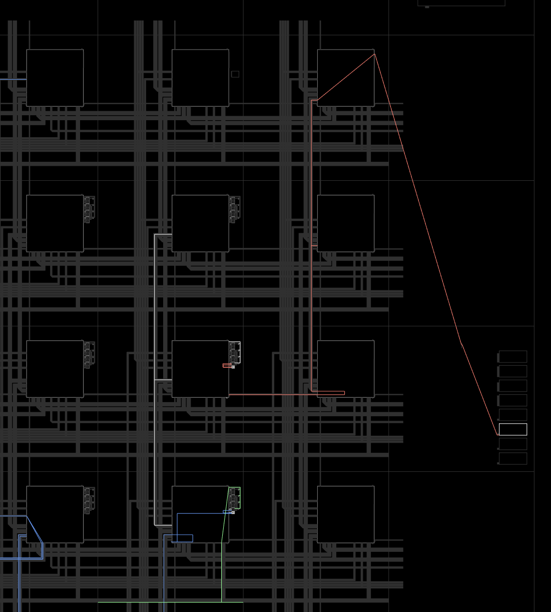
- Place and Route (P&R): Once the design is mapped to the FPGA’s resources, the next step is to determine the physical placement of these resources on the FPGA and the interconnect routing between them. This is a critical step, as the placement and routing can significantly impact the performance and resource utilization of the design. Nextpnr is an open-source P&R tool that can be used with the ECP5 FPGA, and it works in conjunction with Project Trellis, which provides a database of the ECP5’s architecture and bitstream format.
- Bitstream generation: After the P&R process, the final step is to generate the bitstream that will configure the FPGA to implement the design. This bitstream is a binary file that contains the configuration data for the FPGA’s resources and interconnects. Nextpnr and Project Trellis work together to generate the bitstream for the ECP5 FPGA. The “nextpnr-ecp5” command is used to run the Nextpnr tool, which takes the output from Yosys and generates a bitstream using the Project Trellis database.
- Programming the FPGA (configuration): Once the bitstream is generated, it can be programmed onto the ECP5 FPGA using an appropriate programming tool. For example, the open-source tool OpenOCD can be used to program the FPGA via a JTAG interface.
graph TD;
Verilog --> S[[Synthesis\nYosys]];
S --> OD[Optimized design];
OD --> M[[Mapping\nYosys]];
M --> MD[Mapped design];
MD --> PR[[Place and Route\nnextpnr]];
PR --> PLD[Physical layout description];
PLD --> PK[[Generate flashable bitstream\necppack]];
PK --> Bitstream;
Bitstream --> F[[Flash on device\nopenFPGALoader, OpenOCD...]]
High-level synthesis
High-Level Synthesis (HLS) is the process of converting a high-level hardware description language (HDL) design, such as Verilog or VHDL, into a lower-level representation that is suitable for further optimization and mapping to an FPGA or ASIC. The primary goal of HLS is to generate an optimized, technology-independent representation of the design that can be more easily mapped to the target hardware.
HLS involves several sub-processes, including:
- Parsing: The first step in HLS is parsing the input HDL code to create an internal representation of the design. This internal representation is typically an abstract syntax tree (AST) or a similar data structure that captures the structure of the HDL code, including its modules, instances, and hierarchy.
- Elaboration: The next step is elaboration, which involves resolving the design hierarchy, parameterization, and instantiation of modules. The elaboration process creates a flattened representation of the design by expanding instantiated modules and resolving their interconnections. This step is important for analyzing and optimizing the design at the module level and below.
- Behavioral synthesis: Behavioral synthesis focuses on converting the behavioral descriptions of the design (i.e., the algorithmic or functional specifications) into a structural representation that can be more easily optimized and mapped to hardware resources. This process typically involves converting high-level constructs such as loops, conditional statements, and arithmetic operations into a dataflow graph or a control-data flow graph (CDFG). These graphs represent the design at a lower level of abstraction and expose opportunities for optimizations such as pipelining, loop unrolling, and resource sharing.
- Scheduling: Scheduling is the process of assigning operations in the design to specific time steps or clock cycles. This is a critical step in HLS because it determines the latency, throughput, and resource utilization of the design. Scheduling can be performed using various algorithms, such as ASAP (As Soon As Possible), ALAP (As Late As Possible), or more sophisticated techniques that take into account resource constraints and performance goals.
- Resource allocation and binding: Once the operations have been scheduled, the next step is to allocate and bind the required hardware resources, such as functional units (adders, multipliers, etc.), registers, and memories. The resource allocation and binding process involves assigning each operation in the design to a specific functional unit and determining the mapping of variables to registers or memory. This step has a significant impact on the area and power consumption of the final implementation.
- RTL generation: After the scheduling, resource allocation, and binding processes, the HLS tool generates a Register-Transfer Level (RTL) representation of the design. The RTL representation is a lower-level description of the design that can be more easily mapped to an FPGA or ASIC. It typically consists of a netlist of interconnected registers, functional units, and multiplexers, along with the associated control signals.
The output of the HLS process is an optimized RTL design that can be further processed by downstream tools, such as logic synthesis, technology mapping, and place-and-route. The primary advantage of using HLS is that it allows designers to work at a higher level of abstraction, which can improve productivity and enable more complex designs. However, HLS tools may not always generate the most optimized implementations, and manual RTL coding or optimization may still be required for certain designs or performance-critical components.
Optimization
The optimization stage is a crucial part of the process of converting high-level hardware descriptions into a lower-level representation that can be mapped onto FPGAs or ASICs. During optimization, the design is transformed and refined to meet performance, area, and power goals, while ensuring that the functional requirements are maintained. This stage typically involves several types of optimizations, including:
- Constant propagation: This optimization identifies and simplifies expressions containing constants, replacing them with their constant values. This can help reduce the complexity of the design and eliminate unnecessary logic gates.
- Dead code elimination: Dead code refers to portions of the design that have no impact on the output or are never executed. Dead code elimination identifies and removes such redundant parts of the design, which helps to save area and power by eliminating unnecessary resources.
- Boolean simplification: This optimization applies Boolean algebra rules to simplify the logic expressions in the design, reducing the number of gates and interconnections. This can help to minimize the area and delay of the resulting implementation.
- Algebraic simplification: This technique simplifies arithmetic expressions in the design, by applying algebraic identities and arithmetic properties. For example, multiplication by a power of two can be replaced with a shift operation, which is typically more efficient in hardware.
- Common subexpression elimination: This optimization identifies and eliminates redundant computations in the design by reusing the results of identical subexpressions. This can help to reduce the overall complexity of the design and save hardware resources.
- Technology mapping: Technology mapping transforms the design into a representation that is compatible with the target FPGA or ASIC technology. This involves mapping the design to the specific resources available on the target device, such as Look-Up Tables (LUTs), flip-flops, and other specialized components like DSP blocks and memory blocks. Technology mapping also optimizes the design for the target technology by selecting the most suitable primitives and resource configurations.
- Retiming: Retiming is an optimization technique that moves registers across combinational logic boundaries to improve performance or reduce area. This can help to balance the pipeline stages or critical paths, which can improve the overall performance of the design.
- Resource sharing: This optimization technique identifies opportunities to share hardware resources among multiple operations or instances, which can help to save area and power. This is particularly important when mapping the design to an FPGA, where resources such as DSP blocks and memories are limited.
These optimization techniques can be applied in various orders and combinations, depending on the specific design and optimization goals. Some optimizations may be more suitable for certain types of designs or target technologies, and trade-offs may need to be made between performance, area, and power.
In the context of open-source tools like Yosys, many of these optimizations are performed automatically as part of the synthesis process. However, the user can also control or fine-tune the optimizations through various command-line options or synthesis scripts. It is essential to understand and apply the appropriate optimizations to achieve the desired design goals while maintaining the functional requirements of the design.
Mapping
Mapping to FPGA resources is the process of converting the optimized design representation (typically at the Register-Transfer Level, or RTL) into a form that is compatible with the specific resources available on the target FPGA. This process involves determining how the design’s logic functions, storage elements, and other components can be efficiently implemented using the FPGA’s resources. Some of the key resources available on FPGAs include:
- Look-Up Tables (LUTs): LUTs are the primary building blocks of FPGAs, used to implement combinational logic functions. They are essentially small, programmable memory elements that can generate any desired logic function of their inputs. LUTs usually have a fixed number of inputs (e.g., 4-input, 6-input) and can be cascaded or combined to implement more complex functions.
- Flip-flops (FFs): Flip-flops are used to store state information in the design, providing synchronous storage elements for implementing registers, counters, and state machines. FPGAs typically have dedicated flip-flops associated with each LUT, which can be configured to store the output of the LUT or to bypass the LUT and store an external signal.
- Block RAM (BRAM): BRAM is a dedicated memory resource available on FPGAs, used to implement larger memory structures such as buffers, caches, and lookup tables. BRAMs can be configured to support different widths and depths, and multiple BRAMs can be combined to create larger memory structures.
- Digital Signal Processing (DSP) blocks: DSP blocks are specialized resources available on many FPGAs for implementing arithmetic functions, such as multipliers, adders, and accumulators. They are designed to provide higher performance and lower power consumption compared to equivalent implementations using LUTs and flip-flops.
- Input/Output (I/O) blocks: I/O blocks are the interface between the FPGA and external signals. They can be configured to support various I/O standards, voltages, and drive strengths. I/O blocks also often include support for specialized functions, such as clock input and output, analog-to-digital conversion, and high-speed serial interfaces.
During the mapping process, the design’s components are assigned to specific FPGA resources, and the interconnections between these resources are established. This involves:
- Logic synthesis: The RTL design is transformed into a gate-level netlist, which is a representation of the design in terms of gates, flip-flops, and other low-level primitives. This step may involve additional optimizations, such as constant propagation, Boolean simplification, and resource sharing.
- Technology mapping: The gate-level netlist is mapped to the specific resources available on the target FPGA, such as LUTs, flip-flops, and DSP blocks. This step involves selecting the most suitable FPGA primitives and configurations to implement the design’s components while optimizing for performance, area, and power.
- Packing: Packing is the process of grouping the mapped components into larger structures called “tiles” or “clusters” that correspond to the physical resources on the FPGA. For example, LUTs and flip-flops can be packed together into “slices,” which are the basic building blocks of many FPGAs. Packing can help to improve the utilization of FPGA resources and reduce the complexity of the place-and-route process.
In the context of the Lattice ECP5 FPGA and open-source tools like Yosys, the mapping process is performed using the “synth_ecp5” command, which performs logic synthesis and technology mapping specifically for the ECP5’s resources. Once the design is mapped to the ECP5’s resources, it can be passed to the next stage of the implementation process, which is the place-and-route (P&R) step using tools
Place and Route (PNR)
Place and Route (P&R) is a critical stage in the FPGA or ASIC implementation process, following the mapping of the design to the target device’s resources. The primary goal of P&R is to determine the physical placement of the design’s components on the FPGA or ASIC and the interconnect routing between them. The quality of the P&R process has a significant impact on the performance, area, and power consumption of the final implementation. P&R involves two main sub-processes:
- Placement: The placement step determines the physical locations of the design’s components (such as LUTs, flip-flops, and DSP blocks) on the FPGA or ASIC. The objective is to find an optimal placement that minimizes the total wirelength, reduces congestion, and meets performance (timing) constraints. The placement process can be guided by various algorithms, such as simulated annealing, genetic algorithms, or analytical techniques. During placement, the tool also takes into account the target device’s architecture, including the arrangement of resources, the available routing resources, and any other constraints, such as fixed locations for specific components (e.g., I/O pins or clock resources).
- Routing: After the components have been placed, the routing step determines the interconnect paths between them, using the available routing resources (such as routing channels, switches, and wire segments) on the FPGA or ASIC. The goal of the routing process is to find a congestion-free and timing-optimized routing solution that satisfies the design’s performance requirements and minimizes power consumption. Routing can be performed using various algorithms, such as pathfinder, negotiated congestion, or iterative rip-up and reroute techniques.
P&R tools often use a cost function or objective function to guide the optimization process and evaluate the quality of the placement and routing solutions. This function may take into account various factors, such as wirelength, congestion, timing, area, and power consumption. The P&R tool iteratively refines the placement and routing solutions to minimize the cost function, subject to the design constraints and target device’s architectural constraints.
In the context of the Lattice ECP5 FPGA and open-source tools, Nextpnr is a commonly used P&R tool, which works in conjunction with Project Trellis. Project Trellis provides a database of the ECP5’s architecture and bitstream format, enabling Nextpnr to perform P&R specifically for the ECP5 FPGA. To run Nextpnr for ECP5, the “nextpnr-ecp5” command is used, which takes the mapped design output from Yosys as input and generates a placed and routed design suitable for bitstream generation.
During the P&R process, the tool generates various reports and visualizations that help designers analyze the quality of the placement and routing solutions and identify any issues or bottlenecks. These reports may include information about the utilization of FPGA resources, the distribution of wirelengths, the critical path delays, and the timing slack. Designers can use this information to guide further optimization or refinement of the design, either at the RTL level, during the mapping process, or by adjusting P&R constraints and settings.
Bitstream generation
Bitstream generation is the final stage in the FPGA implementation process, following the successful completion of the Place and Route (P&R) step. The bitstream is a binary file that contains the configuration data required to program the FPGA with the designed hardware. This data includes the settings for the FPGA’s programmable resources, such as Look-Up Tables (LUTs), flip-flops, memory blocks, and interconnect routing. The bitstream generation process involves converting the placed and routed design into a format that can be loaded onto the FPGA to configure its resources.
During bitstream generation, the following steps are typically performed:
- Design translation: The placed and routed design is translated into a device-specific representation that includes the settings for the FPGA’s programmable resources. This step involves mapping the design’s components and interconnects to the specific configuration elements of the target FPGA, such as configuration memory cells, programmable switches, and routing multiplexers.
- Bitstream assembly: The translated design is assembled into a bitstream, which is a sequence of binary data that represents the configuration settings for the FPGA’s resources. The bitstream is organized according to the target FPGA’s programming interface and memory organization, and may include additional data, such as error detection codes, synchronization patterns, or configuration commands.
- Bitstream compression (optional): Some FPGA vendors and tools support bitstream compression, which can help to reduce the size of the bitstream and the time required to program the FPGA. Bitstream compression typically involves applying lossless compression algorithms, such as Run-Length Encoding (RLE) or Huffman coding, to the configuration data.
- Bitstream encryption and authentication (optional): In order to protect intellectual property or ensure the security of the design, some FPGA vendors and tools support bitstream encryption and authentication. This involves encrypting the bitstream using a cryptographic algorithm (such as AES) and a secret key, and/or adding an authentication code (such as an HMAC) to the bitstream. The FPGA’s programming interface must support the corresponding decryption and authentication mechanisms to load the encrypted or authenticated bitstream.
In the context of the Lattice ECP5 FPGA and open-source tools, the bitstream generation process is performed using the Project Trellis tools. After the P&R step with Nextpnr, the output is a JSON file that represents the placed and routed design. This file is then passed to the “ecppack” tool, which is part of the Project Trellis suite, to generate the final bitstream. The “ecppack” tool translates the design’s components and interconnects into the ECP5’s configuration elements and assembles the bitstream according to the ECP5’s programming interface and memory organization.
Once the bitstream is generated, it can be loaded onto the target FPGA using a programming tool or interface, such as JTAG, SPI, or an embedded configuration memory. The FPGA reads the bitstream and configures its programmable resources according to the design’s settings, thereby implementing the desired hardware functionality.
Verilog assignments
We have various kinds of assignment in Verilog:
- In clocked blocks (always @(posedge clk ) for example)
- Blocking assignment (led_reg = clk_i)
- Non blocking assignments (led_reg <= clk_i)
- Continuous assignments (assign led_o = clk_i)
Things have to be scheduled by whatever interprets the HDL description of your system.
This is just a simplified view but this is more or less the order of operations in a given module:
- Run all the blocking assignments
- Run the right-hand side(RHS) of non-blocking assignments and schedule the updates of the left hand side
- Update the left-hand-side
- Run the continuous assignments
- Update inputs and outputs
- …
There is an additional mode which is not present on every FPGA but is on the ECP5 that allows you to initialize registers to specific values. Some FPGA don’t have that and will either assign at 0, or even have values random.
You have to think that non-blocking statements may take more cycles to happen than you think (because things have to propagate).
Whereas blocking ones will happen instantly.
Avoid mixing both if you don’t need to (and the result may not be exactly portable from different kinds of FPGA).
ECP5 in details
Main view
This is a symbolic representation of the ECP5 chip on your i5 board (from nextpnr-ecp5 –gui)
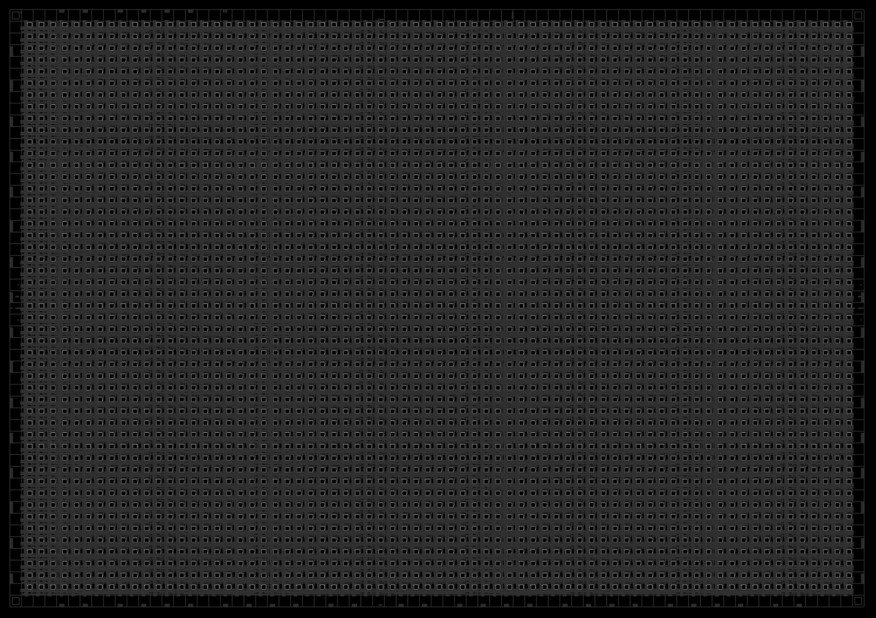
PFU blocks
Each of those numerous squares is a what is called a PFU block:
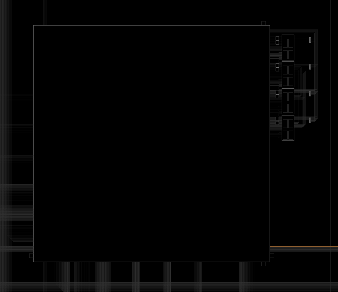
Slices
And each of these blocks contain 4 slices:
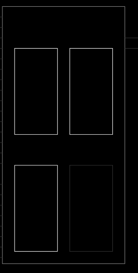 And each of those slices contain 2 LUT4s and 2 registers. They can take multiple configurations like a block of RAM (SRAM), or ROM or be combined to make LUT5,6,7 or 8.
LUTs
Let’s see what a LUT is.
LUT is short for Look-up table. A LUT is a small memory with an address decoder. A LUTn will have 2^n memory cells. So a LUT4 will have 16 memory cells. With 4 wires as its inputs, it can then store 16 different values.
To make a XOR gate you would program a LUT2 as such:
The slices usually contain complex routing systems that allow connecting the LUT, registers and other components of the slice together in various ways.
These are the kind of functions that a single slice can do in an ECP5:
- Addition 2-bit
- Subtraction 2-bit
- Add/Subtract 2-bit using dynamic control
- Up or Down counter 2-bit
- Up/Down counter with asynchronous clear
- Up/Down counter with preload (sync)
- Ripple mode multiplier building block
- Multiplier support
- Comparator functions of A and B inputs
- A greater-than-or-equal-to B
- A not-equal-to B
- A less-than-or-equal-to B
Implementing RAM in an FPGA is pretty costly. To implement 16x4 bits of SRAM, you need 3 slices. For DPRAM (RAM that can be written or read at the same time by two entities), you need 6 slices. That’s why FPGAs often include specific blocks of RAM (BRAM) to reduce the area.
The ECP5 on the i5 (LFE5U-25) is one of the small ones. It has 24K LUTs, 56 blocks of 18 Kbits of system memory (fully enclosed memory system that can do dual port and have their own clocks). 1008 Kbits of embedded memory. 194 Kbits of distributed ram.
It also contains 28 hardware multipliers (18bits by 18 bits).
There are also more advances DSP cores (sysDSP) but they are not handled yet by the OSS tools. If you are interested in helping with the reverse engineering of that, I’m sure the world of ECP5 users would love you very much.
Clocks
sysCLOCK PLLs: The ECP5 FPGA contains four sysCLOCK Phase-Locked Loop (PLL) modules, which can generate a wide range of output frequencies and phase relationships from a single input clock source. They provide flexible clock generation and conditioning features such as frequency synthesis, clock phase shifting, and clock duty cycle control. There are two of those in the ECP5 you have.
DDR-PLLs: In addition to the sysCLOCK PLLs, the ECP5 FPGA also contains two DDR-PLLs specifically designed for high-speed DDR memory interfaces, ensuring accurate clocking for memory operations. There are two of those in the ECP5 you have.
Global Clock Buffers (GCBs): ECP5 FPGA devices feature a global clock network comprising GCBs. These buffers are responsible for distributing low-skew, low-jitter clock signals throughout the FPGA fabric. They help reduce clock skew and minimize clock-to-clock and clock-to-data signal delays.
Clock Multiplexers (MUXes): Clock MUXes are used to select between multiple clock sources for a specific logic element or resource in the FPGA. This allows designers to optimize power consumption and performance by selecting the appropriate clock source for different parts of the design.
Clock Dividers: The ECP5 FPGA also features clock dividers that allow designers to generate multiple, slower clock signals from a single high-speed clock source. This helps in reducing power consumption and optimizing performance for specific logic elements or resources.
Enhanced Logic Array Blocks (E-LABs): E-LABs are the basic building blocks of the ECP5 FPGA, containing programmable logic elements, registers, and memory resources. Each E-LAB can be independently clocked, providing fine-grained control over clock distribution and enabling efficient power management.
Dynamic Clock Gating: The ECP5 FPGA supports dynamic clock gating, which allows designers to selectively enable or disable clock signals to specific regions of the FPGA fabric, reducing power consumption when parts of the design are idle.
Clock and Data Recovery (CDR) circuits: These are used in high-speed serial interfaces such as SERDES to recover clock signals embedded in data streams, ensuring proper synchronization between the transmitter and receiver. But in the ECP5 chip of the colorlight i5 there is no SERDES.
ECP5 routing with blinky
This is the routing of our blink example from lesson 01.
In light blue we see the clock dividing mechanism.
In orange in the top-right that’s our assign led register to led output.
And in green are all the support things (connecting clocks and things together plus a lot of things I have no idea about)
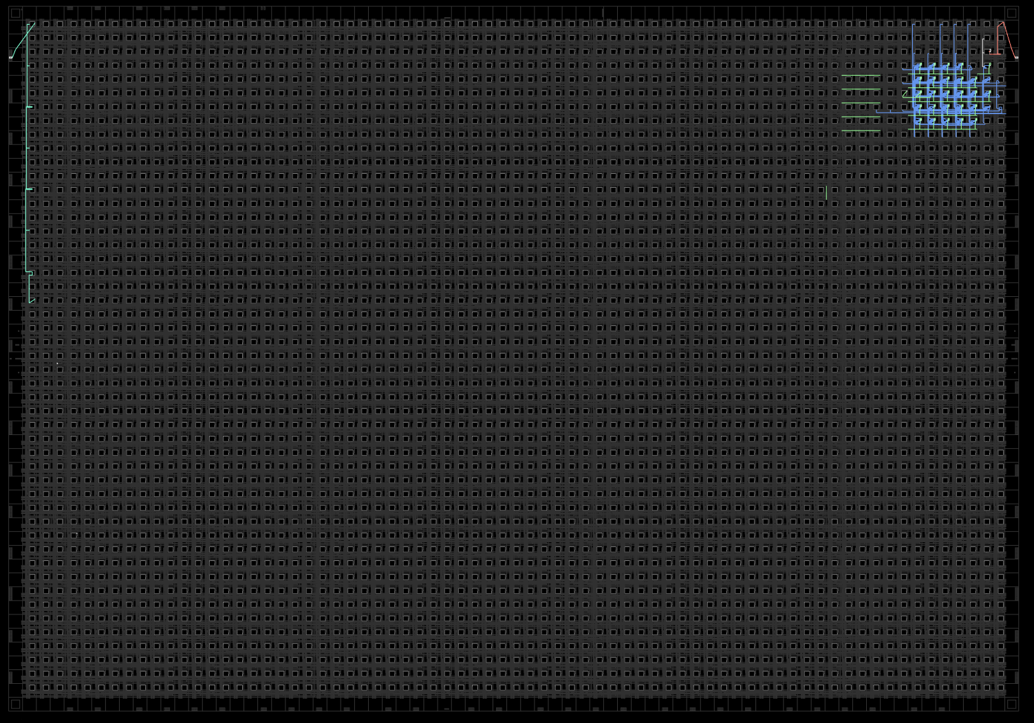
If we zoom in the top right, we can see how the divider network is connected to the led register: